OnseSense Monitoring Station Assembly Guide
OneSense monitoring stations can be configured in a small number of distinct ways to accept the available PCB type equipment deployed.
This document will describe the installation for assembly of a OneSense open space monitor station when using PCB2.0V5 or PCB2.0V6 for multi-sensor applications. For small single input sensing or actuations deployments the information would apply for connection device using PCB0.5V2.
Caution: please read these instructions, guides, manual or information carefully before you commence any integration or work on the installed equipment and follow the instructions given or known as conventions and good trade practice by a suitably qualified industry professional.
The most critical issue in installation and integration is Power Supply that can affect i.e. burn out sensitive electronic components. Ensure that the module is receiving the correct voltage and current as specified in its datasheet.
• Inadequate power can lead to malfunctioning. If uncertain do not apply power and seek advice from your OneSense Partner / Supplier or a suitably qualified technician.
Always power down to conduct maintenance, make configurations change and replacement of PCB / modem / power equipment or similar circumstance.
This supplied equipment is rigorously test and trialled before all supply, however any equipment can be damaged from mishandling or destroyed by improper actions outside the product specification(s) at the integrators sole risk that is beyond any liability of the manufacturer and supplier.
PCB2.0V5
PCB2.0V5 in the 5th iteration of PCB2.0 and incorporates a variety of input and output functions. The range of applied applications are described in the FUNCTION section.
PCB2.02V5 is supplied with firmware that allows the board to be configured for many different application(s). Additional capability and specific connected equipments can be achieved by uploading the appropriate firmware (.bin file) and enabling various pre-loaded device libraries.
PCB Preparation
PCB2.0V5 can be configured for both digital and analog information collection and actions. Digital data is collected via the onboard RS-485 interface while analog information is collected via four (4) independent analog inputs. These analog inputs can be configured to read various voltage levels or count pulses, etc.
The analog inputs can be implemented in different ways to measure various voltage levels in response to necessary parameter(s) to be measured. The configuration adjustments are made by adding the appropriate resistor values into the space provided. See the Analog Input Table.
The PCB firmware translates the voltage level at the I/O input into the relevant value for transmission to the platform.
For instance, a reading of 2.5 vdc could mean a water tank is 40% full or holding 18,000 litres. These reading are adjusted as part of the calibration process for the PCB. The relevant resistors are R23, R24, R25, R26, R31, R35, R36, R42, R43, R44, R45, & R46.
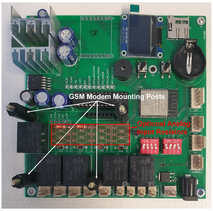 Figure 1 - Unmounted PCB2.0V5
PCB Configuration
Before the PCB can be used, it must be mapped to a OneSense Device which must already exist in the relevant OneSense Tenancy. See Device Creation in the OneSense User Manual.
Mapping is performed using the OneSense phone APP. This procedure uploads the Device Name and the Over-The-Air (OTA) URL that will be used for firmware loading and updates.
PCB Mapping
The PCB can be mapped to a Device or re-mapped to a different Device at any time.
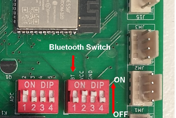
1 – Enable BLE mode on the PCB by switching the BT switch ON. 2 – Power the PCB ON. The PCB will beep and enter BLE mode 3 – Open the OneSense APP and login to the applicable OneSense Tenancy. 4 – Download the Device Key 5 – Download the OTA URL 6 – Select the PCB to be mapped 7 – Press ‘Configure’ to transfer the Device data to the PCB. 8 – If Wi-Fi is to be used, enter the required credentials. 9 – If a mobile network is to be used, enter some ‘dummy’ Wi-Fi credentials. 10- Transfer the data to the PCB 11 – Log out the APP 12 – Switch the BT switch OFF 13 – Restart the PCB. 14 – The PCB is now configured to communicate with the OneSense platform and will accept the OTA upload of its firmware. This is performed in the Operations function on the platform.
Telemetry Transmission
Telemetry is transmitted to the OneSense platform via the onboard Wi-Fi interface. The PCB can also be fitted a GSM mobile network modem for remote application or locations without Wi-Fi.
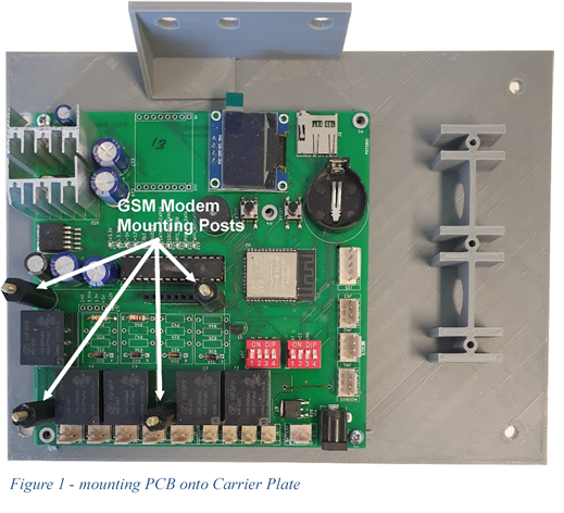
The GSM modem is a piggyback PCB which is fitted above analog input calibration area on the post provided. Note: the posts are not required for Wi-Fi only operation.
Carrier Plate
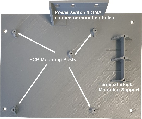
Figure 2 - Bare PCB Carrier Plate
Once the PCB has been prepared it can be fitted to the carrier plate
Mounting the PCB onto the Carrier Plate
Wiring The PCB and Carrier Plate
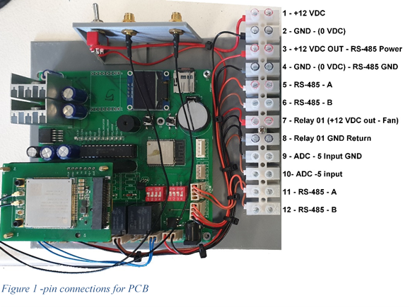
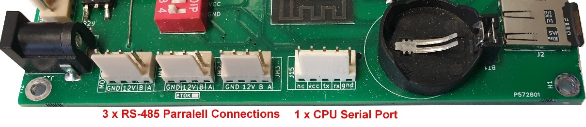
The above example is a typical PCB-2V5 for installation in a remote monitoring station. It is fitted with a GSM modem and wired with one (1) 12 VDC power input, two (2) RS-485 data connections, one (1) 12 VDC power output, one (1) Fan Relay output, and one (1) analog input. Future versions (PCB-3) will have a 50-way edge connector and matching backplane to facilitate more efficient assembly.
Inter Connections
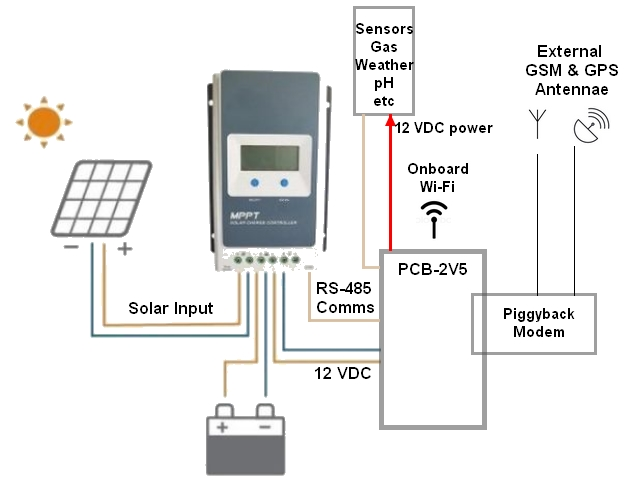
Figure 5 - Typical Wiring Diagram for Remote Monitoring Station
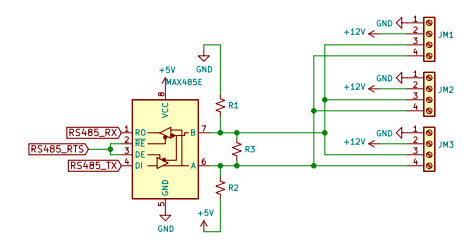
Internal RS-485 Connector Wiring
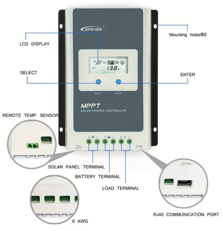
The selected intelligent Solar Controller can communicate with the PCB using the MODBUS protocol over the RS-485 interface and its RJ-45 Ethernet connector. Data is transmitted on the Blue (B signal) and White (A signal) conductors. These wires connect directly to the appropriate PCB terminal block.
External RS-485 connector Wiring
A weather protected RJ-45 connector or a waterproof 4-pin circular chassis mount connector pair is used for external RS-485 connections. This connector provides both power and data connection to external devices. The wire colours shown below are typical but can vary between manufacturers.
Pin Assignment
| Pin | Signal | Typical Sensor Conductor Colour |
|---|---|---|
| 1 | +12vdc | Red |
| 2 | B | Blue/Brown/Green (Depends on supplier) |
| 3 | A | Often yellow |
| 4 | Ground (0vdc) | Black |
Figure 6 - Table 1: External RS-485 Pin Assignment
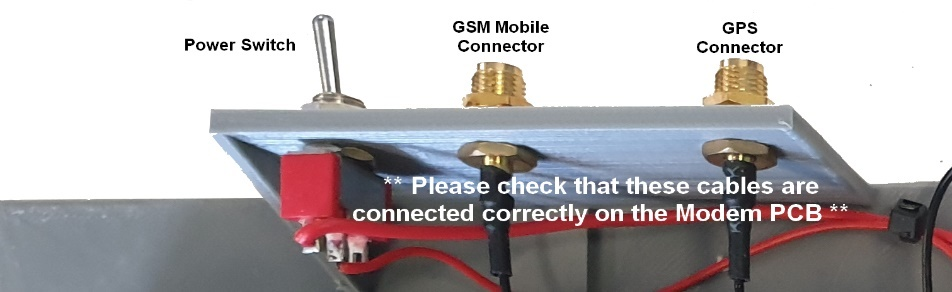
External Antennae Connections
Antennae and Solar Power cables are generally fed through the enclosure's mounting frame and terminated to the appropriate connector within the enclosure.
Solar Array Connections
Three types of Solar Controller are available, Basic, Smart or Smart with OLED display.
Basic Solar Controller
The basic controller provides status information via the user display. It is a low-cost device suitable for standardised system that do not require status information to be remotely available.
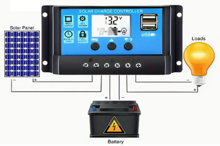
Smart Solar Controller
The smart controller is able to provide status and battery condition information via its RS-485 communications port. The PCB can read the controller’s Holding Registers and send the information to OneSense for display on the Device Dashboard.
Installing the PCB and Carrier Plate
The assembled PCB & carrier plate are fitted into the enclosure as required to suit the physical constrains imposed by the controller type, battery size, and enclosure type. This enclosure would nominally be 400mm height x 300mm width x 200mm depth.
The image below shows an example of the assembly fitted to a field operation site monitoring station. This particular station has a smart solar controller and a 12 volt 25 A hr lithium battery. The station’s battery is charged by the 100 W solar panel that can be seen on this monitoring station display.
Station wiring will vary depending on what options are fitted, its geographic location, and the enclosure material and inclusions.
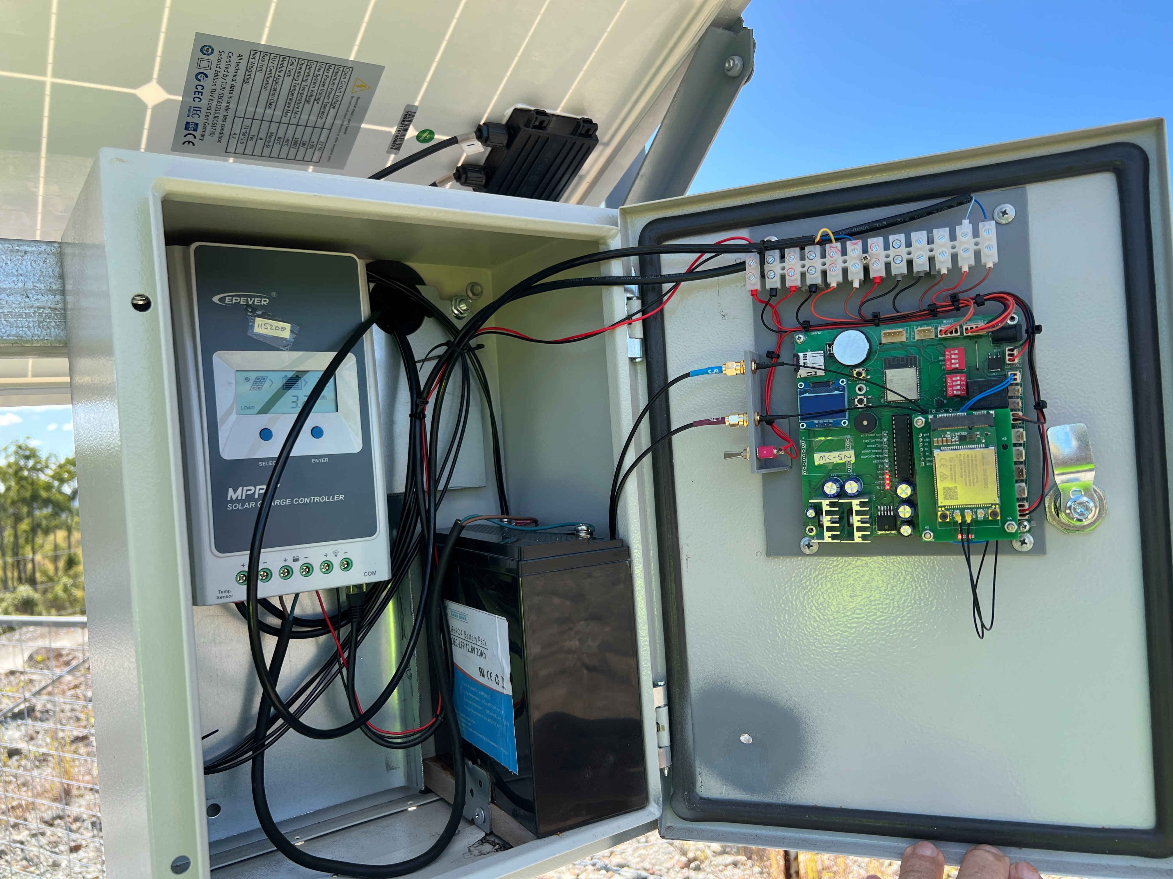
Figure 7 - Internal View of Typical Remote Monitoring Station
This is a typical weatherproof enclosure in this case a steel enclosure which requires external antennas that are free of any shadowing for the GSM and GPRS functions. Non-ferrous enclosures in remote areas may also require external antennae.
Commissioning
Once the station has been assembled and the wiring carefully checked for wiring connections conformity for wiring standard compliance, the station can be powered ON. The following should occur.
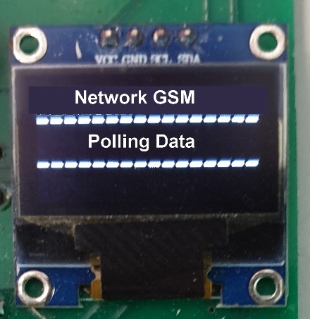
- The PCB power indicators will illuminate and the onboard PCB buzzer will sound.
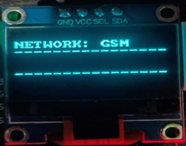
- The OLED display where fitted will show Network Waiting while the PCB attempts to connect to a Wi-Fi network.
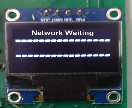
- The PCB will initially attempt to connect to a Wi-Fi network. If the PCB cannot connect after several attempts it will then check for the presence of a GSM modem.
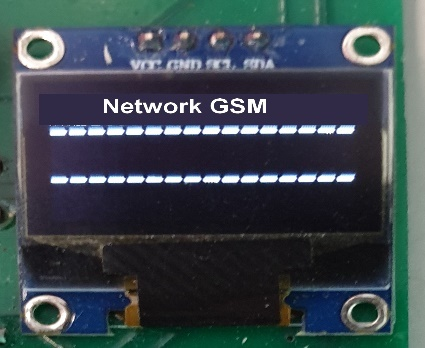
If a modem is present the PCB will attempt to connect to the GSM mobile network if one is available. The PCB will make several attempts to connect to the GSM network. If this is not successful, the PCB will @#$#$%^&.
An active SIM card is required to connect to a GSM mobile network.
If the PCB can establish a connection to either a Wi-Fi or GSM network, it will start collecting data and send it to the platform.
Where the installation has an available Lora gateway at a suitable internet transfer station plus an installed Lora network modem, the system will then proceed to make a wireless connection and start collecting data and send it to the platform.
The network connection and PCB activity will be shown on the display. Sensor telemetry should be viewable on the Device’s generic Platform Dashboard within a few minutes.
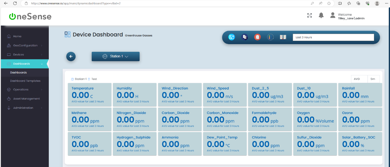
Dashboards
Dashboards can be created as required. In this instance the dashboard shows the average Greenhouse Gas levels recorded during the last three (3) hours.
Maximum and Minimum vales can also be displayed over user selected time periods.
Digital Interface Connections
This description refers to PCB2.0V5. PCB0.5V2 uses a similar design but with fewer connections available.
RS-485
Analog Interface Connections
* Relay Outputs
Relay one (1) provides a 12Vdc output when activated. It is intended as a cooling-fan switch and as such operates differently from the other relays. If a cooling fan is not fitted Relay-1’s output can be used as a low-power switchable +12Vdc supply. If used for this purpose a 500 mA fuse should be included on the load side of the PCB.
Relays two (2) to five (5) provide isolated dry contact switching for external loads.
ADC Inputs
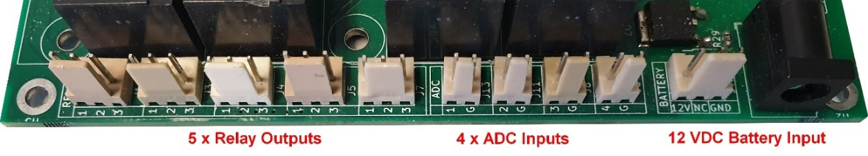
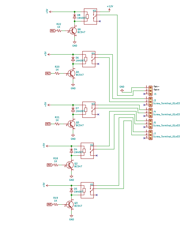 Figure 9 -ADC input schematic diagram showing all available inputs
Analog Input Configuration Options
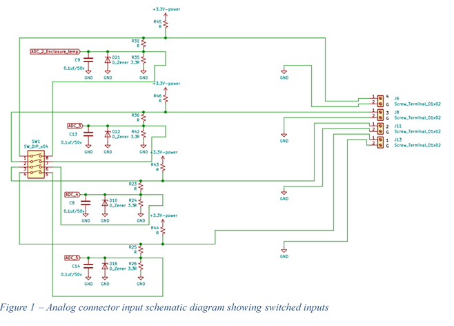
- Single analog input describing the various configuration options available on PCB2.0V5.
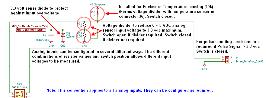
These configurations must of course be matched to the PCB firmware and calibrated to the needs of the site.
For instance, when a pressure transducer is being used to monitor the water level in a storage tank, the PCB firmware much read the appropriate ADC input and have the correct calibration data entered via the Device’s Dashboard CONFIG menu.
The maximum transducer voltage must also be limited via the voltage divider network.
Calibration of Water Level Transducer
The water level transducer will generally provide a 0.5 ~ 4.5 vdc output. The range is linear from zero (0.5 vdc) to full scale (4.5vdc). The transducer’s specification will indicate the maximum depth that it can measure and these values must be entered into the Device Configuration table on OneSense.
| Parameter | Value |
|---|---|
| Resistor Value R1* | 1 |
| Resistor Value R2* | 2.2 |
| Tank Volume | 40000 |
| Tank Empty Voltage | 0.5 |
| Tank Full voltage | 4.5 |
- Note-1: These values form a voltage divider to reduce the incoming sensor voltage. They must match the resistors installed on the PCB. Refer to Analog Input Calibration Options
- Note-2: PCB0.5V2 and PCB2.0V5 have minor differences, please refer to the appropriate schematic for up-to-date information
The above values are for a transducer with a maximum pressure reading of two (2) metres. The volume will be determined by the user after calculating the maximum storage available.
The maximum storage available is determined the diameter and the number of tanks that are interconnected. The data is entered into the tenancy’s Device Configuration table.

PCB2.0V6
This document outlines how an assembly of a OneSense device(s) with PCB2.0V6. As the sixth iteration of PCB2.0, PCB2.0V6 features various input and output functions. The board is provided with initial operating firmware that allows for initial integration. The veracity of the equipment provided for uploading application functions derived from the appropriate .bin file and enabling various pre-loaded device libraries.
PCB Components
Main PCB board
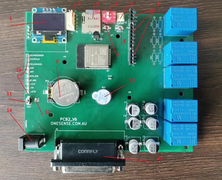
Figure 11: Main PCB2.0V6 board
- OLED
- Flash pins
- SD card slot
- ADC dip switch
- Enclosure Temperature sensor
- Lora-GSM Communication board connector
- Boot pin
- Reset pin
- RTC battery pad
- LED indicators
- User/Bluetooth switch
- User/Bluetooth Indicator
- Buzzer
- Barrel jack connector for 12V input from external source
- Edge Connector
Backplane:
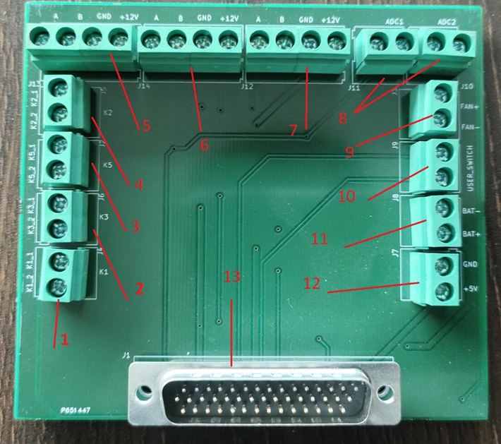 Figure 12 - Backplane
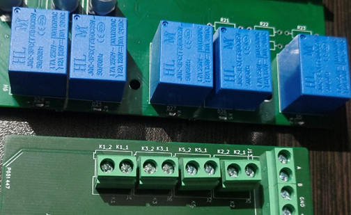
- Relay K1
- Relay K3
- Relay K5
- Relay K2
- Modbus Connector terminal
- Modbus Connector terminal
- Modbus Connector terminal
- ADC 1 and ADC 2 Connector terminal
- Cooling Fan Connector terminal
- User Switch terminal
- External connection provided battery switching
- 5V output terminal: can be used to output a 5V power.
- Edge connector
PCB2v6 main board connected with backplane
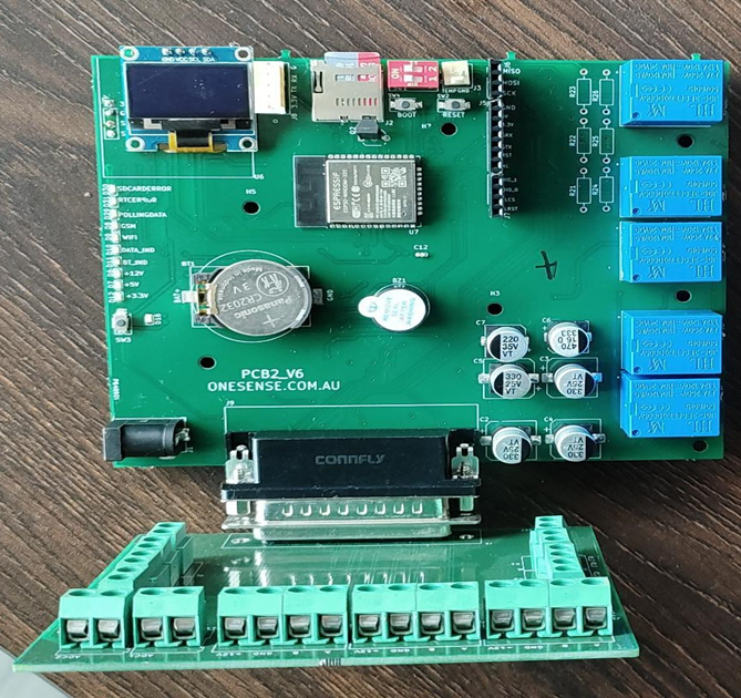 Figure 13 - Backplane connected to Main PCB2.0V6
Comm board connected with PCB2.0V6 main board
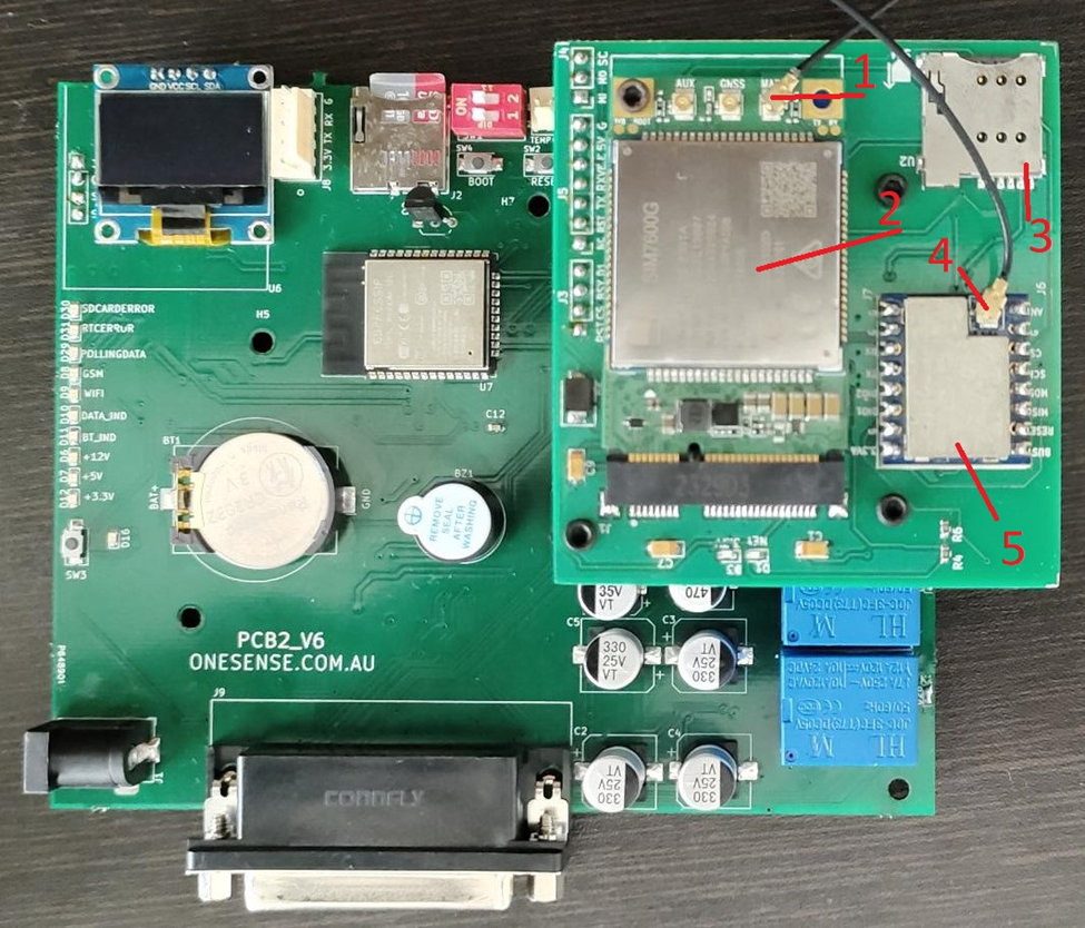 Figure 14 - Comm board connected to Main PCB2V6
Antenna connector for GSM
- GSM modem
- GSM SIM slot
- Antenna connector for LORA
- Lora Module
PCB Configuration
Before using the PCB, it must be mapped to an existing OneSense Device within the relevant OneSense Tenancy. This mapping process is done using the OneSense phone app. During this procedure, the Device Name, Device primary key, OneSense hub host name, and Wi-Fi SSID and Password are uploaded, which are necessary for firmware loading and updates.
Prerequisites
- Insert the SD card.
- Insert the coin battery for the RTC.
- Connect all the necessary sensors.
- If using GSM or LoRa for network communication, connect the Comm board to the main PCB-2V6 board.
- Connect the power supply (12V DC supply from battery or 230/12V adapter).
PCB Mapping
The PCB can be mapped to a Device or re-mapped to a different Device at any time.
* Mapping Procedure Details: Steps to Configure the PCB
- Power On the PCB: Use a 12V battery supply or a 12V adapter from a 230V/12V power source.
- Check Bluetooth Status:
- If the PCB has not been configured before, it will automatically turn on Bluetooth. You can verify this by checking the BLE indicator on the board.
- If the PCB is already mapped to another device, press and hold the user/BLE switch for 5 seconds to enter BLE mode.
- Open OneSense Android Phone App: Launch the OneSense app and log in to the relevant OneSense Tenancy.
- Copy Device Key: Copy the Device key from the OneSense app.
- Connect to PCB via Bluetooth: Scan for the Bluetooth device and connect to the PCB that needs to be mapped.
- Transfer Device Data: Press ‘Configure’ in the app to transfer the Device data to the PCB.
- Enter Wi-Fi Credentials: If Wi-Fi is to be used, enter the required Wi-Fi credentials.
- Enter Dummy Wi-Fi Credentials: If a mobile network is to be used, the WiFi credentials requirement still has to be applied so enter some non-specific Wi-Fi credentials.
- Transfer Data to PCB: Complete the data transfer to the PCB.
- Log Out of Configuration App: Log out of the OneSense app.
- Restart PCB: Restart the PCB.
- Verify Configuration: The PCB is now configured to communicate with the OneSense platform.
You can perform OTA updates using the Device update feature on the OneSense platform.
Telemetry Transmission
Telemetry is transmitted to the OneSense platform via the onboard Wi-Fi interface. For remote applications or locations without Wi-Fi, the PCB can be equipped with a GSM mobile network modem. Additionally, it features a LoRa network for sending telemetry if Wi-Fi or GSM is not available. The GSM modem and LoRa are mounted on a piggyback PCB that fits above the PCB2.0V6 main board.
- Note: The posts shown are not required for Wi-Fi only operation.
Commissioning
Once the station has been assembled and the wiring carefully checked and in strict accordance with the specification(s), the station can be powered ON.
The following should occur.
 • The PCB power indicators will illuminate and the buzzer will sound.
 • The OLED display will show Network Waiting while the PCB attempts to connect to a Wi-Fi network.
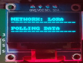
Initially, the PCB will make attempts to connect to a Wi-Fi network. If unsuccessful after several attempts, it will proceed to check for the presence of a GSM modem. In the presence of a modem, the PCB will attempt to establish a connection with the GSM mobile network. If GSM connectivity is unavailable, the PCB will then attempt to connect to the LoRa network. Upon successful connection to any of these networks, the PCB will proceed to transmit telemetry data via the established network according to the embedded protocol.
• An active SIM card is required to connect to a GSM mobile network that is a tenant requirement.
Once the PCB successfully establishes a connection to either a Wi-Fi, GSM network or LORA, it initiates data collection and transmission to the platform. The network connection status and PCB activity are displayed on the screen. Within a few minutes, sensor telemetry should be visible on the Platform Dashboard of the device.
Enclosure Temperature sensor
The temperature sensor can be connected to the pin located near the DIP switch, boot, and reset buttons.
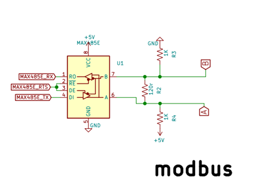
Modbus Connector
The PCB2.0V6 features three Modbus connection terminals accessible from the backplane, as illustrated in Figure 2. Sensors should be connected to these terminals as follows: • connect the sensor's 12V line to the 12V pin, • the ground (GND) to the GND pin, • Pin A to the A terminal, and • Pin B to the B terminal.
ADC Terminal
The ADC terminal can be utilized for connecting ADC sensors, with the PCB2.0V6 accommodating the connection of up to two ADC sensors. These sensors are also connected to the backplane, as illustrated in Figure 2, demonstrating the terminals designated for ADC sensor connection.
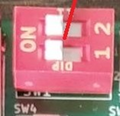
- Note: Make sure to turn on the DIP switch for ADC 1 and 2.
Relays in PCB2.0V6
There are a total of 5 Relays in PCB2.0V6 board. Relay one (K1) functions by providing a 12 VDC output upon activation. Its primary purpose is to serve as a cooling fan switch, operating distinctively from the remaining relays. In the absence of a cooling fan, the output of Relay-1 can be utilized as a low-power switchable +12 VDC supply.
The remaining four (4) relays offer isolated dry contact switching capabilities for external loads.
Turn ON BLE in PCB2.0V6
Bluetooth is utilized for configuring the PCB, allowing users to map new PCB to device or modify the device already mapped to the PCB and configure Wi-Fi credentials via BLE. To activate BLE on PCB2.0V6, press and hold the BLE/user switch for 5 seconds until the BLE indicator illuminates. Subsequently, open the OneSense configuration app to proceed with device configuration.
PCB0.5 V2 Configuration
Before the PCB can be used, it must be mapped to a OneSense Device which must already exist in the relevant OneSense Tenancy. See Device Creation in the OneSense User Manual.
Mapping is performed using the OneSense android based smartphone APP (Config 5.2). This procedure uploads the Device Name and the Over-The-Air (OTA) URL that will be used for firmware loading and updates.
PCB Mapping
The PCB can be mapped to a Device or re-mapped to a different Device at any time. Please see section – Mapping Procedure Detail
- To activate the PCB, initially power it on. Upon the first boot, the system will seamlessly transition into BLE mode.
- However, for subsequent reinitializations, it's essential to hold down the user switch for a duration of five seconds. This action prompts the system to enter BLE mode. While maintaining the user switch in this position, observe the associated LED, which will remain continuously illuminated, serving as confirmation that the switch is operating as intended and Blue LED turns on when BLE is On.
- Open the OneSense APP and login to the applicable OneSense Tenancy.
- Select the PCB to be mapped.
- Download the Device Key
- Press ‘Configure’ to transfer the Device data to the PCB.
- If Wi-Fi is to be used, enter the required credentials.
- If a mobile network is to be used, enter any set of Wi-Fi credentials.
- Transfer the data to the PCB.
- Log out of the APP.
- The PCB is now configured to communicate with the OneSense platform and will accept the OTA upload of its firmware. This is performed in the Operations function on the platform.
- When reinitializing, pressing the user switch for five seconds is necessary to enter the system into BLE mode. While holding the user switch button, the associated LED will remain steadily lit, indicating that the switch is functioning properly.
- After entering in to BLE mode follow the same procedure as mentioned above.
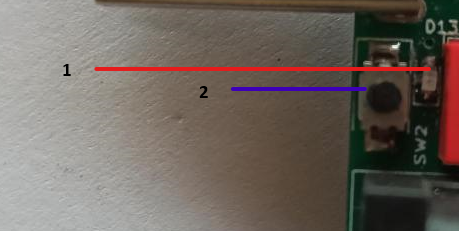
USER SWITCH WITH LED
- LED
- User switch
LED remains steadily lit when pressing the user switch, showing it is operating.
Telemetry Transmission
Telemetry is transmitted to the OneSense platform via the onboard Wi-Fi interface. The PCB can also be fitted a GSM mobile network modem for remote application or locations without Wi-Fi.
The GSM modem is a piggyback PCB which is fitted above analog input calibration area on the post provided. Note: the posts are not required for Wi-Fi only operation.
Carrier Plate

Once the PCB has been prepared it can be fitted to the carrier plate
PCB mounting holes of PCB0.5v2
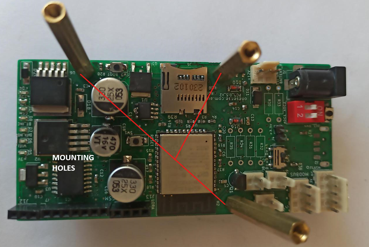 Figure 16 - PCB mounting holes of PCB0.5V2
TROUBLE SHOOTING PCB2.0V6
- Power Supply: Ensure that the module is receiving the correct voltage and current as specified in its datasheet. Inadequate power can lead to malfunctioning. If uncertain do not apply power and seek advice from a suitably qualified technician. a. Always power down to conduct maintenance, make configurations change and replacement of PCB / modem / power equipment etc.
RESET BUTTON
The reset button can be used in various scenarios to resolve issues with the PCB and to perform other useful functions:
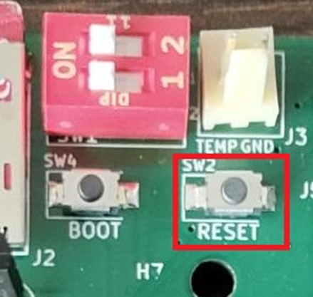
Using the Reset Button
• No PCB response: When the PCB does not respond to inputs or actions, press the reset button to reboot the system. • No BLE function: If the Bluetooth function does not activate after attempting to use the BLE/user switch, use the reset button to reset the PCB and try again. • Restarting the System: Use the reset button to quickly restart the device, especially after software updates or configuration changes. • Recovering from Errors: Press the reset button to recover from software crashes or error states. • Clearing Temporary Issues: Use the reset button to clear temporary issues affecting the device's performance. • Returning to Initial State: Reset the device to return it to a known initial state for easier troubleshooting. • Testing and Debugging: Utilize the reset button during development and testing to quickly reset the device and test various scenarios.
TROUBLE SHOOTING MODBUS / COMMUNICATIONS ISSUES
SD Card Troubleshooting
- Power Cycle and Reinsert the SD Card • Power Off: Turn off the PCB. • Remove and Inspect: Remove the SD card and inspect it for any physical damage or debris on the contacts. • Reinsert: Carefully reinsert the SD card, ensuring it is properly seated in the slot. • Power On: Turn the PCB back on and check if the SD card is recognized.
- Format the SD Card • Backup Data: If possible, back up any important data or log from the SD card using a computer. • Format: Format the SD card using a computer. • Reinsert: Insert the formatted SD card back into the PCB and power on the system.
Modem (GSM & LoRa communication board)
- Check the power LED on Comm board: If the power led is not turned on, it indicates the GSM modem does not have enough power to operate. • Check the status of the power supply from the illumination of the first LED • Verify the connection to the PCB board. • Verify the connection to the Modem / comm board. If the power LED is on, it means that the module is receiving power and is turned on.
- Check the network LED: If the second network LED remains continuously turned on, then the modem is searching for an internet connection.
- Verify network connection: If the second network LED commences to display long duration flashing, the modem is attempting to connect to an identified GSM network signal. When a suitable signal and signal strength is available, the status of the network LED will be indicated by commencement of short duration flashing indication an internet connection is established but there is no indication of that signal strength. To ascertain the available network signal diagnostics, a readily available network app can be used independently of the OneSense configuration.
- If the power LED is on and the network LED is not displaying the second red LED: It generally indicates one of the following scenarios: • No Network Connection: The module is powered on but not connected to a cellular network. This could be due to a lack of signal and signal strength, • Check SIM Card: Ensure that a valid SIM card is properly inserted into the module. Verify that the SIM card is active. Potentials issues may involve network registration, and sufficient payment balance with a suitable data plan. • If the integrations cannot be established for any of the above circumstances, typically hardware issues or wiring layout may require investigation. Should there be an issue with the module firmware preventing it from initializing the network component properly, an OTA can be carried out to ensure the correct configuration has been uploaded.
TROUBLE SHOOTING EQUIPMENT INTEGRATION ISSUES
- Typically connected equipment have some orientation needs like: a. north facing for sensors and solar panel (in southern hemisphere) b. other equipment may need direct line of sight or near line of sight. c. other equipment have distance limitations for their operation.
- Faulty Wiring and Connections a. Loose Connections: Ensure all connections are secure. Loose wires can cause intermittent communication failures. b. Damaged Cables: Inspect cables for cuts, nicks, or other physical damage that might disrupt the signal. c. Incorrect Wiring: Double-check that the wiring matches the network topology requirements, especially the polarity and grounding for RS-485 networks.
- No Response from Slave Device: a. Verify the slave address. b. Check communication settings. c. Ensure proper connection between Modbus sensor and PCB.
- Hardware Compatibility a. Incompatible Devices: Ensure all devices on the network are compatible with the same Modbus protocol and communication parameters. b. Firmware Versions: Devices with outdated or incompatible firmware may not communicate correctly. Ensure all devices are updated to the latest firmware versions. c. Connection issues: ensure that various equipment requirements are applied for the operating specification like analogue or RS485 connections.
TROUBLE SHOOTING SIGNAL TRANSMISSION ISSUES
Internal aerial or external aerial use
Check signal performance: The setup of connection hardware equipment is dependent on additional issues such as environmental factors for signal reception and signal sending like the circumstance of a Faraday’s Cage effect on signal transmissions. At times, the signal strength can be improved simply by the pointing of the transmission or avoiding obstruction from other equipment or enclosures.
Signal Strength: Ensure that the module is in an area with good cellular signal reception. You might need to connect an external antenna or a signal amplifier to improve signal strength.
Check correct Antenna Connection: The supplied connection equipment typically has two antenna connections, one being GSM and the other being GPRS. The modem comes with two small connection cable with a screw connector that is an engineered fit to the Modem mini terminals. a. GSM is typically a horizontal transmission unless satellite LEO is needed and installed. Check that the antenna is securely connected to the module at the correct terminal point and the terminal point for the GSM connection lead. A loose or disconnected antenna can prevent the module from detecting the network. b. GPRS is the second connection point to the Modem. The GSM aerial may have been supplied with a combined external or internal aerial or may have a separate positioning aerial. It is required that this aerial or whatever type used is directly orientated to the sky and without obstruction to connect with positioning satellites. • Check the GSM modem separately by connecting to ss.com software and then send AT commands to verify the working of modem. Common commands:
   AT -> Check the response of AT command
   AT+CSQ -> Check the network connectivity
   AT+CPING="www.google.com",1,1,64,1000,10000,255 ->
Recheck the internet connectivity!